Cwazibeh
On this page, you find all documents, package deals, and flashcards offered by seller cwazibeh.
- 31
- 0
- 0
Community
- Followers
- Following
31 items

E-FSM-OVERVIEW
ystem has n inputs and m outputs and 2pow(k) states. • The STATE of a sequential circuit is a collection of state variables whose value at any time contain all the information about the past necessary to account for the circuits future behavior. • A circuit with k binary state variables has 2pow(k) possible finite states. • Sequential circuits are also named Finite-state machines because the sequential logic circuit that implements them can be in only a fixed number of possible states. ...
- Class notes
- • 16 pages •
ystem has n inputs and m outputs and 2pow(k) states. • The STATE of a sequential circuit is a collection of state variables whose value at any time contain all the information about the past necessary to account for the circuits future behavior. • A circuit with k binary state variables has 2pow(k) possible finite states. • Sequential circuits are also named Finite-state machines because the sequential logic circuit that implements them can be in only a fixed number of possible states. ...

STATE-MINIMIZATION-ASSIGNMENT
Motivation: lower cost- number of states is closely related to the complexity of the resulting circuit; – fewer flip-flops in implementations. – more don’t cares in next state logic. – fewer gates in next state logic. – Simpler to design with extra states then reduce later. • Several Methods of state Reduction
- Class notes
- • 47 pages •
Motivation: lower cost- number of states is closely related to the complexity of the resulting circuit; – fewer flip-flops in implementations. – more don’t cares in next state logic. – fewer gates in next state logic. – Simpler to design with extra states then reduce later. • Several Methods of state Reduction

-SYNCRONOUS SEQUENTIAL-DESIGN
Use clock pulses as one of the inputs of the flip-flops. • They seldom show instability problems and their timing is easily broken down into independent discrete steps, each of which can be analysed separately. • When a clock pulse is not active, the feedback loop is broken, the flipflop outputs cannot change even if the combinational logic driving their inputs change in value.
- Class notes
- • 36 pages •
Use clock pulses as one of the inputs of the flip-flops. • They seldom show instability problems and their timing is easily broken down into independent discrete steps, each of which can be analysed separately. • When a clock pulse is not active, the feedback loop is broken, the flipflop outputs cannot change even if the combinational logic driving their inputs change in value.

E-SYNCRONOUS SEQUENTIAL-ANALYSI
Use clock pulses as one of the inputs of the flip-flops. • They seldom show instability problems and their timing is easily broken down into independent discrete steps, each of which can be analysed separately. • When a clock pulse is not active, the feedback loop is broken, the flipflop outputs cannot change even if the combinational logic driving their inputs change in value.
- Study guide
- • 27 pages •
Use clock pulses as one of the inputs of the flip-flops. • They seldom show instability problems and their timing is easily broken down into independent discrete steps, each of which can be analysed separately. • When a clock pulse is not active, the feedback loop is broken, the flipflop outputs cannot change even if the combinational logic driving their inputs change in value.

TUT3
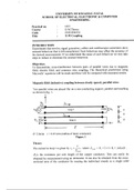
ontinuous bits, and generates an output of ‘1’ if the sequence (1011) is detected. Draw the timing diagrams for an input sequence of 01011011010100. 2. Design a synchronous sequential circuit with two inputs xi, yi and one output zi. The output is the sum of the inputs. Design using: a) D FF b) JK FF and c) T FF. Using your own combination of inputs draw timing diagrams to confirm your circuits. 3. Design a majority checker that compares the number of 1s with the number of 0s in the 3-bit in...
- Class notes
- • 7 pages •
ontinuous bits, and generates an output of ‘1’ if the sequence (1011) is detected. Draw the timing diagrams for an input sequence of 01011011010100. 2. Design a synchronous sequential circuit with two inputs xi, yi and one output zi. The output is the sum of the inputs. Design using: a) D FF b) JK FF and c) T FF. Using your own combination of inputs draw timing diagrams to confirm your circuits. 3. Design a majority checker that compares the number of 1s with the number of 0s in the 3-bit in...

TUT2
ven one JK and one D FF. Design a circuit that reads as inputs continuous bits, and generates an output of ‘1’ if the sequence (1011) is detected. Draw the timing diagrams for an input sequence of 01011011010100. 2. Design a synchronous sequential circuit with two inputs xi, yi and one output zi. The output is the sum of the inputs. Design using: a) D FF b) JK FF and c) T FF. Using your own combination of inputs draw timing diagrams to confirm your circuits. 3. Design a majority checker that...
- Exam (elaborations)
- • 4 pages •
ven one JK and one D FF. Design a circuit that reads as inputs continuous bits, and generates an output of ‘1’ if the sequence (1011) is detected. Draw the timing diagrams for an input sequence of 01011011010100. 2. Design a synchronous sequential circuit with two inputs xi, yi and one output zi. The output is the sum of the inputs. Design using: a) D FF b) JK FF and c) T FF. Using your own combination of inputs draw timing diagrams to confirm your circuits. 3. Design a majority checker that...
TEST1
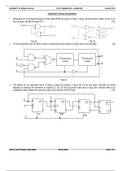
hematics for a Flip-Flops Company of their latest IP/OP are shown in Figure 1 below. Fill the function Tables 1a and 1b on the next page. Indicate the type of FF For the sequential circuit of Figure 2 below, complete the timing diagram of Figure Q2 on the next page. [10] The signals for the sequential circuit of Figure 3 below are shown in Figure Q3 on the next page. Complete the timing diagrams by drawing the waveforms of signals Q1, Q2, Q3 and Q4 whose initial value is logic zero. Assu...
- Exam (elaborations)
- • 3 pages •
hematics for a Flip-Flops Company of their latest IP/OP are shown in Figure 1 below. Fill the function Tables 1a and 1b on the next page. Indicate the type of FF For the sequential circuit of Figure 2 below, complete the timing diagram of Figure Q2 on the next page. [10] The signals for the sequential circuit of Figure 3 below are shown in Figure Q3 on the next page. Complete the timing diagrams by drawing the waveforms of signals Q1, Q2, Q3 and Q4 whose initial value is logic zero. Assu...